1

Physical Design Engineer Jobs in Phoenix, AZ (NOW HIRING)

I/O Design Engineer

Chandler, AZ ยท On-site

$125 - $150/hr

Work closely with layout teams to oversee physical design and verification. * Build Verilog ... MS or PhD in Electrical Engineering. * 6+ years of I/O or analog circuit design experience. * Deep ...

Work closely with layout teams to oversee physical design and verification. * Build Verilog ... MS or PhD in Electrical Engineering. * 6+ years of I/O or analog circuit design experience. * Deep ...

Work closely with layout teams to oversee physical design and verification. * Build Verilog ... MS or PhD in Electrical Engineering. * 6+ years of I/O or analog circuit design experience. * Deep ...

IC Packaging Design Engineer

Chandler, AZ ยท On-site

$138K/yr

We are seeking experienced IC Packaging Design Engineers to support advanced semiconductor ... Develop and implement physical design and layout solutions for advanced IC packages. * Perform ...

ASIC Physical Designers - IV

Chandler, AZ ยท On-site

$133K - $137K/yr

... , Creative and Marketing talent. Akraya has extensive experience supporting Fortune 500 and hot ... CW will assist the Physical Design Team in executing RF and analog custom layout. * Tasks include ...

Principal Engineer, CAD

Tempe, AZ ยท On-site

$160K - $230K/yr

... Signal Simulations, IC Physical Design layout, CAD tool customizations, Linux Support ... The Principal CAD Engineer will also interface with EDA Tool Vendors and have responsibilities for ...

Design Engineer

Scottsdale, AZ ยท On-site

$150 - $200/hr

As a Principal Design Engineer located in Scottsdale, Arizona, you will have the opportunity to ... physical or mental disability, medical condition, genetic information, military or veteran status ...

Silicon Packaging Design Engineer

Phoenix, AZ ยท On-site

$135K/yr

Key Responsibilities: - Design and implement physical layout and routing of silicon interposers and ... Engineering, or a STEM related field Experience listed above should be in the following:

As a Principal Design Engineer located in Scottsdale, Arizona, you will have the opportunity to ... physical or mental disability, medical condition, genetic information, military or veteran status ...

As a Principal Design Engineer located in Scottsdale, Arizona, you will have the opportunity to ... physical or mental disability, medical condition, genetic information, military or veteran status ...

Showing results 21-40

Physical Design Engineer information

See Phoenix, AZ salary details

$94.3K

$140.5K

How much do physical design engineer jobs pay per year?

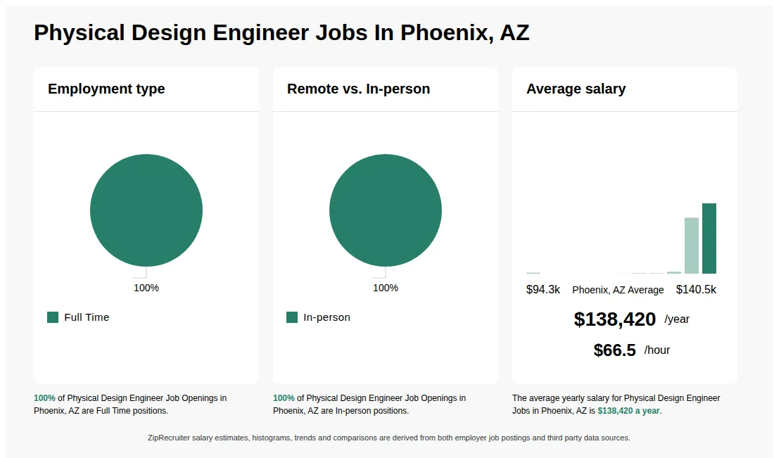
As of Sep 7, 2026, the average yearly pay for physical design engineer in Phoenix, AZ is $138,420.00, according to ZipRecruiter salary data. Most workers in this role earn between $135,000.00 and $139,000.00 per year, depending on experience, location, and employer.

What is a physical design engineer?

A Physical Design Engineer is responsible for transforming logical circuit designs into a physical layout that can be manufactured as an integrated circuit (IC). They focus on key aspects like floor planning, placement, clock tree synthesis (CTS), routing, and timing closure while ensuring power and performance optimization. They work with Electronic Design Automation (EDA) tools and collaborate with front-end designers to meet design specifications. The role requires proficiency in tools such as Cadence, Synopsys, or Mentor Graphics and knowledge of processes like ASIC or SoC design.

What are the typical daily responsibilities of a physical design engineer?

As a Physical Design Engineer, your daily responsibilities typically include taking logical circuit designs and translating them into physical layouts, performing floorplanning, placement, and routing of blocks, and conducting timing closure and verification. You will use specialized EDA tools to ensure that designs meet performance, power, and area requirements, collaborating closely with design, verification, and manufacturing teams. The role also involves resolving design issues, optimizing chip layouts, and preparing design data for fabrication. Working in this position provides exposure to advanced technology nodes and the opportunity to contribute directly to the development of cutting-edge semiconductor products.


What are the key skills and qualifications needed to thrive as a physical design engineer?

To thrive as a Physical Design Engineer, you need a solid background in electrical engineering, experience with ASIC or SoC design methodologies, and a deep understanding of digital circuit fundamentals. Proficiency with EDA tools like Synopsys, Cadence, or Mentor Graphics, as well as familiarity with scripting languages and industry certifications, is highly valued. Attention to detail, effective teamwork, and strong problem-solving skills are essential soft skills for this role. These qualifications are crucial as they enable efficient chip design, ensure successful project delivery, and foster productive collaboration in complex engineering environments.

What are the most commonly searched types of Physical Design Engineer jobs in Phoenix, AZ?

The most popular types of Physical Design Engineer jobs in Phoenix, AZ are:

What are popular job titles related to Physical Design Engineer jobs in Phoenix, AZ?

For Physical Design Engineer jobs in Phoenix, AZ, the most frequently searched job titles are:

What job categories do people searching Physical Design Engineer jobs in Phoenix, AZ look for?

The top searched job categories for Physical Design Engineer jobs in Phoenix, AZ are:

What cities near Phoenix, AZ are hiring for Physical Design Engineer jobs?

Cities near Phoenix, AZ with the most Physical Design Engineer job openings:

Infographic showing various Physical Design Engineer job openings in Phoenix, AZ as of August 2026, with employment types broken down into 61% Full Time, and 39% Contract. Highlights an 100% In-person job distribution, with an average salary of $138,420 per year, or $66.5 per hour.

Senior Advanced Packaging / Substrate Design Engineer (2.5D/3D Chiplets)

black.ai

Tempe, AZ โ€ข On-site

$150 - $200/hr

Other

Medical, Dental, Vision, Retirement, PTO

Posted 6 days ago


Key responsibilities

  • Lead the physical design, floor planning, pad/bump allocation, and complex routing of multi-layer organic substrates and 2.5D/3D interposer architectures.

  • Drive die-to-package and package-to-board co-design, collaborating with ASIC, signal integrity, and power integrity engineering teams.

  • Work with substrate foundries and OSATs to ensure design-for-manufacturing (DFM) compliance, handling build-up sequences, microvia rules, and coreless substrate constraints.


Job description

About Syenta

Syenta is pioneering a new era in semiconductor manufacturing with our groundbreaking Localised Electrochemical Manufacturing (LEM) technology. Our manufacturing products build cutting edge advanced packaging for the semiconductor industry by combining patterning and metallization into a single tool. We do that by achieving high-speed, high-resolution metallization at significantly lower costs and energy use, while minimizing emissions and waste.

Founded in Australia, our growing footprint in the US represents a key milestone in our journey. We are building a world-class team where seasoned engineers and ambitious emerging talent collaborate to solve some of the toughest challenges in semiconductor manufacturing.

About the Role

We are seeking a Senior Advanced Packaging Design Engineer to drive the physical design, layout, and implementation of next-generation heterogeneous integration platforms. In this role, you will be at the forefront of semiconductor innovation, designing complex 2.5D and 3D organic substrate interposers, high-density RDLs, and chiplet architectures for high-performance computing (HPC) and AI applications.

If you have a passion for pushing the boundaries of physical layout, die-to-package co-design, and advanced substrate manufacturing, we want you on our team.

Responsibilities
  • Physical Layout & Floor planning: Lead the physical design, floor planning, pad/bump allocation, and complex routing of multi-layer organic substrates and 2.5D/3D interposer architectures.
  • Co-Design Execution: Drive die-to-package and package-to-board co-design, collaborating closely with ASIC design, signal integrity (SI), and power integrity (PI) engineering teams.
  • Design Verification: Run and resolve advanced Design Rule Checks (DRC), Layout Versus Schematic (LVS), and electrical rule checks specific to fine-pitch packaging technologies.
  • DFM & Manufacturing Collaboration: Work directly with substrate foundries and OSATs to ensure design-for-manufacturing (DFM) compliance, handling build-up sequences, microvia rules, and coreless substrate constraints.
  • Reliability Optimization: Coordinate with thermal and mechanical engineering teams to mitigate warpage, CTE mismatch, and thermo-mechanical stress in organic substrate designs.
Requirements
  • Education: B.S. or M.S. in Electrical Engineering, Computer Engineering, Materials Science, or a related technical discipline.
  • Experience: 5+ years of hands-on experience in semiconductor packaging layout, substrate design, or physical verification.
  • Domain Knowledge: Deep understanding of 2.5D/3D IC integration, chiplet architectures, silicon bridges/interposers, and advanced organic substrate technologies (ABF build-up, fine-pitch routing).
  • EDA Tool Proficiency (Must-Have): Proven mastery of industry-standard advanced packaging EDA tools, including:
    • Synopsys: 3DIC Compiler, Icepak and/or Flotherm
    • Cadence: Allegro Package Designer Plus / Innovus
    • Siemens (Mentor): Xpedition Substrate Integrator / Calibre
  • Analysis Awareness: Familiarity with power integrity, signal integrity, and thermal-mechanical modeling tools (e.g., Ansys Redhawk,HFSS).
  • Deep expertise in high-speed signal design, including mitigation of crosstalk, reflections, and impedance mismatches
  • Solid foundational knowledge across electrical, materials, thermal, and/or mechanical engineering disciplines
  • Strong analytical and problem-solving skills, with the ability to operate effectively in a fast-paced, cross-functional environment
Why Choose Syenta?

Weโ€™re passionate about building a diverse, people-first company. We believe that our culture of collaboration and mutual respect fuels the kind of innovation that can redefine an industry.

What We Offer
  • Competitive salary
  • Early-stage equity opportunities
  • Potential 401(k) and other benefits
  • Comprehensive health, dental, and vision coverage plans, supported by Company
  • Professional Growth โ€“ Weโ€™re scaling fast, so responsibilities can expand significantly in tandem with the business
  • Team Events โ€“ Annual company event in Australia to collaborate and celebrate
  • Work-Life Balance โ€“ Flexible leave policies and an understanding that meaningful work can coexist with a fulfilling personal life
  • 15 days PTO and 10 days sick leave

Syenta is an Equal Opportunity Employer. We do not discriminate on the basis of race, color, religion, sex, sexual orientation, gender identity, national origin, disability, protected veteran status, age, or any other characteristic protected by law.

#J-18808-Ljbffr