2

Remote Pcb Design Jobs in California (NOW HIRING)

US - Remote Job Title: Core Engineering - Design Engineer V PCB Layout Engineer, AR Product Team As a PCB Layout Engineer on Meta's AR Product Team, you will be responsible for driving world-class ...

$134K - $175K/yr

Company Description REMOTE - MUST BE WILLING TO BE LOCATED IN SOUTHERN CALIFORNIA - PREFERRED ... System-level power architecture design, Schematic and PCB layout review , especially for power ...

$134K - $175K/yr

REMOTE - MUST BE WILLING TO BE LOCATED IN SOUTHERN CALIFORNIA - PREFERRED ORANGE COUNTY (LA and San ... System-level power architecture design, Schematic and PCB layout review , especially for power ...

Embedded Software Engineer

Long Beach, CA ยท On-site +1

$118K - $198K/yr

Experience with fundamental hardware components on PCB and their analysis tools. Ability to write ... Remote #LI-MZ1 #UEV What you'll do... Design and implement software running on a distributed ...

Embedded Software Engineer

Long Beach, CA ยท On-site +1

$100K - $168K/yr

Experience with fundamental hardware components on PCB and their analysis tools. Ability to write ... Remote #LI-MZ1 #UEV What you'll do... Design and implement software running on a distributed ...

next page

Showing results 1-20

Remote Pcb Design information

What is a Remote PCB Design job?

A Remote PCB Design job involves designing printed circuit boards (PCBs) from a remote location using specialized software. Engineers or designers collaborate with teams online, creating schematics, layouts, and optimizing designs for manufacturing. This role requires proficiency in PCB design tools like Altium, Eagle, or KiCad and knowledge of electrical engineering principles. Remote PCB designers often work as freelancers or for companies offering flexible work arrangements. Effective communication and experience with design for manufacturing (DFM) are also essential in this role.

What are the key skills and qualifications needed to thrive in the Remote Pcb Design position, and why are they important?

To thrive as a Remote PCB Designer, you need a strong background in electronics engineering, circuit design, and PCB layout principles, often supported by a degree in electrical engineering or a related field. Proficiency with industry-standard EDA tools like Altium Designer, Eagle, or KiCAD and familiarity with IPC standards or relevant certifications is crucial. Excellent communication, problem-solving skills, and self-motivation are vital for collaborating with remote teams and meeting project deadlines. These capabilities are essential to deliver reliable, manufacturable PCB designs while working independently in a distributed work environment.


What are the biggest challenges of working as a Remote PCB Designer, and how can they be managed?

Working remotely as a PCB Designer often means collaborating with engineers, manufacturers, and clients across different locations and time zones, which can make communication and feedback loops more complex. Staying organized, using version control systems, and maintaining detailed documentation are key to ensuring your designs stay aligned with project requirements. Proactively scheduling regular check-ins and utilizing efficient communication tools helps build rapport and quickly resolve issues. By developing strong project management habits and remaining responsive, remote PCB designers can successfully overcome these challenges and keep projects moving smoothly.

What are the most commonly searched types of Pcb Design jobs in California? The most popular types of Pcb Design jobs in California are:
What job categories do people searching Remote Pcb Design jobs in California look for? The top searched job categories for Remote Pcb Design jobs in California are:
What cities in California are hiring for Remote Pcb Design jobs? Cities in California with the most Remote Pcb Design job openings:
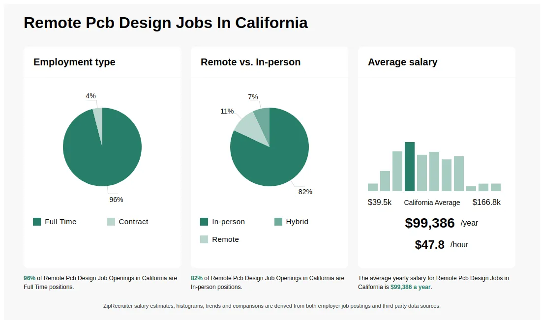
Infographic showing various Remote Pcb Design job openings in California as of July 2026, with employment types broken down into 87% Full Time, 9% Part Time, 1% Temporary, and 3% Contract. Highlights an 87% Physical, 3% Hybrid, and 10% Remote job distribution.
Design Engineer V

Design Engineer V

Infotech Sourcing

Sunnyvale, CA โ€ข On-site, Remote

Other

Re-posted 13 days ago


Job description

Request ID: 69851-1
Duration: 5 months with possible extension

Location: US - Remote

Job Title: Core Engineering - Design Engineer V
Job Description: PCB Layout Engineer, AR Product Team
As a PCB Layout Engineer on Metaโ€™s AR Product Team, you will be responsible for driving world-class, complex PCB layouts that incorporate cutting-edge component and stack-up technologies. A core focus of this role is implementing miniaturization solutions within AR product designs. You will collaborate closely with internal electrical and mechanical engineers, DFM, SiPi, and other layout and library teams, as well as external suppliers.
RESPONSIBILITIES
Project Management & Execution:
Manage multiple complex layout projects, providing timely status reports within Meta systems.
Lead designs from kick-off through tape-out, encompassing rigid, rigid-flex, and flex PCBs for both product and non-product/test projects.
Proactively schedule and drive project meetings (Kick-off, Placement, Constraint, and Design Reviews) to ensure design verification using Meta's Design Traveler document.
Create and modify engineering tool project templates, meta-data, configuration data, and rules.
Technical Expertise & Problem Solving:
Apply a solid understanding of electrical engineering principles, particularly for power distribution, high-speed circuits, and RF signals.
Identify project execution risks or slowdowns proactively and collaborate with managers and/or technical program managers to propose alternative PCB development workflow solutions.
Understand and propose practical fit and function solutions related to miniaturization concepts.
Cross-Functional Collaboration & Supplier Engagement:
Proactively partner with EE Leads, Mechanical Engineering, TPMs, and other cross-functional teams (XFNs) to resolve design issues.
Work with internal DFM engineers to confirm supplier requirements at project launch.
Engage with external suppliers and Supplier Quality/Process Engineering (SQE/PE) to resolve DFM issues and ensure high-yield builds.
MINIMUM QUALIFICATIONS
8+ years of experience in complex PCB Design.
5+ years of experience using Allegro PCB Design Tools (version 23.1 or newer).
Strong understanding of the mechanical aspects of electronics design.
Excellent communication skills.
Proficiency with Microsoft Office tools.
PREFERRED QUALIFICATIONS
BS in Electrical Engineering.
3+ years of experience implementing miniaturization solutions in dense form-factor designs (e.g., wearable products, mobile phone design).


Must-Have Skills 1. Senior-level experience with Cadence Allegro (v21). 2. Rigid-flex and flexible circuit design experience. 3. HDI (high-density interconnect) PCB design experience. 4. Strong overall PCB layout/design background for complex boards.

Nice-to-Have Skills 5. Manufacturing/process exposure (overseeing or supervising manufacturing processes; design-for-manufacturability mindset). 6. Production efficiency / continuous improvement (identify solutions to improve production efficiency). 7. Strong communication & collaboration (verbal/written communication + team player; helpful when coordinating design + manufacturing