1

Wafer Fab Process Engineer Jobs (NOW HIRING)

Senior Wafer Fab Engineer

Salem, NH ยท On-site

$103K - $134K/yr

The Senior Fabrication Engineer will manage the wafer processing operation in a semi-automated wafer fab with several manual operations involved, direct oversight of individual processes and ...

Be Seen First

Job Overview: We are seeking a dynamic and detail-oriented Wafer Fab Equipment Engineer ... Your expertise will ensure that manufacturing processes run smoothly, efficiently, and safely ...

As a Wafer Fab Technician, you would be expected to: ยท Have had experience as an operator in a ... all processing. ยท Identify any malfunctioning equipment and generate maintenance request. ยท ...

Be Seen First

Job Overview: We are seeking a dynamic and detail-oriented Wafer Fab Equipment Engineer ... Your expertise will ensure that manufacturing processes run smoothly, efficiently, and safely ...

Semi Mfg Technician 2

Sunnyvale, CA ยท On-site

$33K - $62K/yr

Execute wafer fab processes with precision, adhering to all specifications and documented procedures. * Collaborate effectively with Production and Wafer Fab Engineering Teams to resolve production ...

Execute wafer fab processes with precision, adhering to all specifications and documented procedures. * Collaborate effectively with Production and Wafer Fab Engineering Teams to resolve production ...

You will collaborate closely with engineers, production teams, and fellow operators to ensure ... Execute wafer fab processes with precision, adhering to established protocols and standards.

Semiconductor Wafer Fab * Photolithography, Wet Etch, Dry Etch, Plating, Lapping, Polishing ... Interact with engineering for process training and execution of non-standard work instructions on ...

Semiconductor Wafer Fab * Photolithography, Wet Etch, Dry Etch, Plating, Lapping, Polishing ... Interact with engineering for process training and execution of non-standard work instructions on ...

Wafer Fab Equipment Engineer

Goleta, CA ยท On-site

$113K - $151K/yr

As part of the Uncooled Detector (Focal Plane Array) Low-Rate Production team, the Wafer Fab ... The Equipment Engineer will be a liaison between process and maintenance providing hands-on ...

Support the wafer fab engineering and operations teams to develop, control and optimize wafer fabrication processes * Work in teams to scale PIC wafer fabrication processes to larger wafer sizes ...

Semi Mfg Technician 2

Sunnyvale, CA ยท On-site

$34K - $63K/yr

You will collaborate closely with engineers, production teams, and fellow operators to ensure ... Execute wafer fab processes with precision, adhering to established protocols and standards.

next page

Showing results 1-20

Wafer Fab Process Engineer information

See salary details

$49.5K

$92K

$142.5K

How much do wafer fab process engineer jobs pay per year?

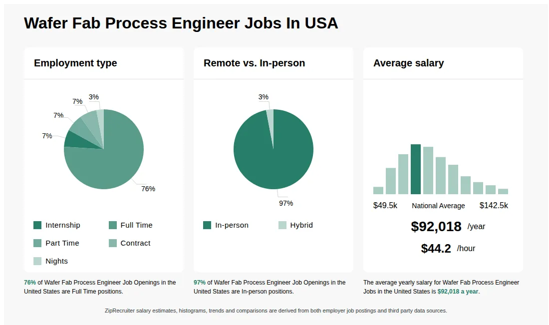
As of Jul 18, 2026, the average yearly pay for wafer fab process engineer in the United States is $92,018.00, according to ZipRecruiter salary data. Most workers in this role earn between $74,500.00 and $103,000.00 per year, depending on experience, location, and employer.

What are some typical challenges faced by Wafer Fab Process Engineers, and how do they overcome them?

Wafer Fab Process Engineers often encounter challenges such as maintaining stringent process control, minimizing defects, and optimizing yield within complex manufacturing environments. They tackle these issues by rigorously analyzing process data, implementing corrective actions, and working closely with equipment technicians and quality teams to fine-tune procedures. Continuous learning and adaptability are crucial, as advances in semiconductor technology require regular updating of skills and methods. Collaboration with cross-functional teams is essential to proactively identify and resolve production problems, ensuring the consistent delivery of high-quality semiconductor products.

What are the key skills and qualifications needed to thrive in the Wafer Fab Process Engineer position, and why are they important?

To thrive as a Wafer Fab Process Engineer, you need a solid background in materials science, semiconductor processing, and a degree in engineering or a related field. Experience with process control systems, SPC software, and familiarity with cleanroom protocols and fab equipment is highly valued. Strong analytical thinking, problem-solving skills, and effective teamwork and communication abilities will set you apart. These capabilities ensure that you can optimize manufacturing processes, maintain high product yield, and collaborate efficiently in a fast-paced, technology-driven environment.

What is a Wafer Fab Process Engineer job?

A Wafer Fab Process Engineer is responsible for developing, optimizing, and maintaining semiconductor fabrication processes in a cleanroom environment. They work with photolithography, etching, deposition, and other wafer-processing techniques to ensure high yield and efficiency. Their role includes troubleshooting process deviations, collaborating with cross-functional teams, and implementing improvements to enhance production quality and reliability.

More about Wafer Fab Process Engineer jobs
What cities are hiring for Wafer Fab Process Engineer jobs? Cities with the most Wafer Fab Process Engineer job openings:
What are the most commonly searched types of Wafer Fab Process Engineer jobs? The most popular types of Wafer Fab Process Engineer jobs are:
What states have the most Wafer Fab Process Engineer jobs? States with the most job openings for Wafer Fab Process Engineer jobs include:
Infographic showing various Wafer Fab Process Engineer job openings in the United States as of July 2026, with employment types broken down into 2% Locum Tenens, 93% Full Time, 2% Part Time, and 3% Contract. Highlights an 87% Physical, 4% Hybrid, and 9% Remote job distribution, with an average salary of $92,018 per year, or $44.2 per hour.
Senior Wafer Fab Engineer

Senior Wafer Fab Engineer

GPD Optoelectronics

Salem, NH โ€ข On-site

$103K - $134K/yr

Full-time

Posted 8 days ago


Job description

We are scaling tomorrow's world, TODAY! We continue to expand our team, a team is shaping the future of our industry and share our passion to reveal the invisible! GPD Optoelectronics Corp. is seeking a Senior Fabrication Engineer. The Senior Fabrication Engineer will manage the wafer processing operation in a semi-automated wafer fab with several manual operations involved, direct oversight of individual processes and operators, and ongoing process optimizations. Also, the ideal candidate will be familiar with more advanced manufacturing technologies/equipment and will help guide ongoing upgrades to the facility. This full-time, exempt role will report to the COO, and will be located at our Salem, NH facility. *** Preference will be given to candidates located within a commutable distance to Salam, NH. Essential Responsibilities: โ€ข Wafer Fab Process Engineering - Process Development for improved process yield, cycle time, and overall throughput. โ€ข III-V wafer fabrication for Photonics, especially InGaAs & Germanium strongly preferred. โ€ข Front End Process: Photolithography, optical coatings, wet chemical processing, metallization, RIE & PECVD thin film deposition โ€ข Back-end Process: Grinding, Lapping, Polishing, Saw, Scribe โ€ข Data-centric approach for design, process control, and improvements โ€ข Ability to forecast and implement upgrades for increased volume and new product production. Involves both capex and process innovation. โ€ข Strong collaboration, relationship management, and interpersonal skills โ€ข Possess Company values of honesty, integrity, respect, commitment and open to change while modeling the Company Core Principles in all activities โ€ข Ability to foster collaborative, cross department relationships to meet common objectives โ€ข Problem solving ability with an organized & analytical approach โ€ข Evaluate and optimize existing processes and procedures โ€ข Lean or Six Sigma experience โ€ข Able to follow MIL-STD requirements, cleanroom protocol, and specific product specifications โ€ข Chemical safety - Engagement in compliance as well as continuous improvement initiatives. Education, Requirements, and Experience: โ€ข Engineering or Physics degree (B.S or greater) and extensive semiconductor fabrication experience. Photodetector and III-V material experience desired. โ€ข Able to meet requirements to work with ITAR and US export restricted items โ€ข Lean or Six Sigma experience is beneficial. MISC: โ€ข Able to lift up to 75lbs โ€ข Travel may be required GPD provides equal employment opportunities to all employees and applicants for employment and prohibits discrimination and harassment of any type without regard to race, color, religion, age, sex, national origin, disability status, genetics, protected veteran status, sexual orientation, gender identity or expression, or any other characteristic protected by federal, state or local laws. This policy applies to all terms and conditions of employment, including recruiting, hiring, placement, promotion, termination, layoff, recall, transfer, leaves of absence, compensation and training. About GPD At GPD Optoelectronics, we believe that by operating with integrity and trust we drive constant organizational improvement, which strengthens our relationships with our employees and customers. Customer success remains our highest priority, so we strive to deliver high-quality products on time, and provide unparalleled service, responsiveness, and collaboration. Founded in 1973 as Germanium Power Devices Corp, we began by making high-quality germanium transistors. Since the early 1980's we have earned our place as a trusted manufacturer of both germanium and indium gallium arsenide photodiodes. We are located in Salem, NH.
GPD Optoelectronics is expanding! Do you have an unwavering commitment to continuous improvement? Do you share the passionate belief that we must always strive to do better? Based out of Salem, NH, our team members are design-oriented, customer-focused, and work hard to engineer custom solutions for every client's needs. If you have an eye for detail and share our passion for the photonics industry, come join our team of professionals who are dedicated to advancing tomorrow's photo detector technology!