Experience with ASIC design flows and methodology of static timing analysis. * Knowledge of ... Google's mission is to organize the world's information and make it universally accessible and ...
Experience with ASIC design flows and methodology of static timing analysis. * Knowledge of ... Google's mission is to organize the world's information and make it universally accessible and ...
... ASIC RTL design, with a focus on clocking, reset, or timing-critical RTL development. * Design ... We empower Google customers with breakthrough capabilities and insights by delivering AI and ...
... ASIC RTL design, with a focus on clocking, reset, or timing-critical RTL development. * Design ... We empower Google customers with breakthrough capabilities and insights by delivering AI and ...
Experience architecting RTL solutions and with ASIC synthesis flows. * Cross-functional engagement ... We empower Google customers with breakthrough capabilities and insights by delivering AI and ...
Experience architecting RTL solutions and with ASIC synthesis flows. * Cross-functional engagement ... We empower Google customers with breakthrough capabilities and insights by delivering AI and ...
... Google . Responsibilities * Understand the overall application of the chip, proposing and developing improvements in overall design. * Design and document one or more blocks of an ASIC, including ...
... Google . Responsibilities * Understand the overall application of the chip, proposing and developing improvements in overall design. * Design and document one or more blocks of an ASIC, including ...
We empower Google customers with breakthrough capabilities and insights by delivering AI and ... Develop SystemVerilog RTL to implement logic for ASIC products according to established coding and ...
We empower Google customers with breakthrough capabilities and insights by delivering AI and ... Develop SystemVerilog RTL to implement logic for ASIC products according to established coding and ...
... Google labs, power, and safety equipment. Regular development and processing of engineering ... Knowledge of ASIC cooling solution stack-ups, their structural behavior, and reliability. About the ...
... Google labs, power, and safety equipment. Regular development and processing of engineering ... Knowledge of ASIC cooling solution stack-ups, their structural behavior, and reliability. About the ...
Experience with ARM-based SoCs, interconnects, and ASIC methodology. Preferred qualifications ... Google's mission is to organize the world's information and make it universally accessible and ...
Experience with ARM-based SoCs, interconnects, and ASIC methodology. Preferred qualifications ... Google's mission is to organize the world's information and make it universally accessible and ...
Experience in design automation, architecting RTL solutions and ASIC Synthesis flows. About the job ... We empower Google customers with breakthrough capabilities and insights by delivering AI and ...
Experience in design automation, architecting RTL solutions and ASIC Synthesis flows. About the job ... We empower Google customers with breakthrough capabilities and insights by delivering AI and ...
Silicon Validation Engineer, Google Cloud
Sunnyvale, CA · On-site
$138K - $198K/yr
... silicon design or semiconductors (digital design, silicon validation, computer architecture ... Experience with high‑speed interfaces, ASIC interfaces, memory systems (HBM), power system ...
Silicon Validation Engineer, Google Cloud
Sunnyvale, CA · On-site
$138K - $198K/yr
... silicon design or semiconductors (digital design, silicon validation, computer architecture ... Experience with high‑speed interfaces, ASIC interfaces, memory systems (HBM), power system ...
corporate_fare Google place Sunnyvale, CA, USA About the job In this role, you'll work to shape the ... experience in ASIC RTL design, with a focus on clocking, reset, or timing‑critical RTL ...
corporate_fare Google place Sunnyvale, CA, USA About the job In this role, you'll work to shape the ... experience in ASIC RTL design, with a focus on clocking, reset, or timing‑critical RTL ...
corporate_fare Google place Sunnyvale, CA, USA Mid * Bachelor's degree in Electrical Engineering ... Experience architecting RTL solutions and with ASIC synthesis flows. * Cross-functional engagement ...
corporate_fare Google place Sunnyvale, CA, USA Mid * Bachelor's degree in Electrical Engineering ... Experience architecting RTL solutions and with ASIC synthesis flows. * Cross-functional engagement ...
Experience with high speed interfaces, ASIC interfaces, memory systems (HBM), aor power system ... Design, develop, operate, and maintain software based validation tests. Information collected and ...
Experience with high speed interfaces, ASIC interfaces, memory systems (HBM), aor power system ... Design, develop, operate, and maintain software based validation tests. Information collected and ...
Senior Design and Integration Engineer, Cloud TPU
Sunnyvale, CA · On-site
$163K - $237K/yr
Experience in design automation, RTL architecture, and ASIC synthesis flows. Compensation US: $163 ... Google is proud to be an equal opportunity and affirmative action employer. We are committed to ...
Senior Design and Integration Engineer, Cloud TPU
Sunnyvale, CA · On-site
$163K - $237K/yr
Experience in design automation, RTL architecture, and ASIC synthesis flows. Compensation US: $163 ... Google is proud to be an equal opportunity and affirmative action employer. We are committed to ...
You will work with Application-Specific Integrated Circuit (ASIC), Field Programmable Gate Array ... Google is proud to be an equal opportunity and affirmative action employer. We are committed to ...
You will work with Application-Specific Integrated Circuit (ASIC), Field Programmable Gate Array ... Google is proud to be an equal opportunity and affirmative action employer. We are committed to ...

Technical Program Manager, Infrastructure
San Jose, CA · On-site
$2.0K/mo
Strong technical knowledge in ASIC design, hardware platforms, and software integration ... Experience using program management tools and methodologies such as Google Workspace and JIRA.
Technical Program Manager, Infrastructure
San Jose, CA · On-site
$2.0K/mo
Strong technical knowledge in ASIC design, hardware platforms, and software integration ... Experience using program management tools and methodologies such as Google Workspace and JIRA.
Technical Program Manager, Infrastructure
San Jose, CA · On-site
$2.0K/mo
Strong technical knowledge in ASIC design, hardware platforms, and software integration ... Experience using program management tools and methodologies such as Google Workspace and JIRA.
Technical Program Manager, Infrastructure
San Jose, CA · On-site
$2.0K/mo
Strong technical knowledge in ASIC design, hardware platforms, and software integration ... Experience using program management tools and methodologies such as Google Workspace and JIRA.
Technical Program Manager, Infrastructure
San Jose, CA · On-site
$2.0K/mo
Strong technical knowledge in ASIC design, hardware platforms, and software integration ... Experience using program management tools and methodologies such as Google Workspace and JIRA.
Quick apply
Technical Program Manager, Infrastructure
San Jose, CA · On-site
$2.0K/mo
Strong technical knowledge in ASIC design, hardware platforms, and software integration ... Experience using program management tools and methodologies such as Google Workspace and JIRA.
RTL Design Engineer, Machine Learning Accelerators
Sunnyvale, CA · On-site
$138K - $197K/yr
Learn more about benefits at Google . * Understand the overall application of the chip, proposing and developing improvements in overall design. * Design and document one or more blocks of an ASIC ...
RTL Design Engineer, Machine Learning Accelerators
Sunnyvale, CA · On-site
$138K - $197K/yr
Learn more about benefits at Google . * Understand the overall application of the chip, proposing and developing improvements in overall design. * Design and document one or more blocks of an ASIC ...
... ASIC firmware development using C and C . About the job Like Google's own ambitions, the work of a ... design, networking, security, data compression, user interface design; the list goes on and is ...
... ASIC firmware development using C and C . About the job Like Google's own ambitions, the work of a ... design, networking, security, data compression, user interface design; the list goes on and is ...
Experience in ASIC or SoC bring-up, debugging, or functional verification. * Experience leading ... to design and test for the next generations of chips. You will be a key member of the team that ...
Experience in ASIC or SoC bring-up, debugging, or functional verification. * Experience leading ... to design and test for the next generations of chips. You will be a key member of the team that ...
Google Asic Design information
See salary details
$94K - $103.8K
16% of jobs
$103.8K - $113.6K
3% of jobs
$113.6K - $123.5K
4% of jobs
$126.3K is the 25th percentile. Wages below this are outliers.
$123.5K - $133.3K
6% of jobs
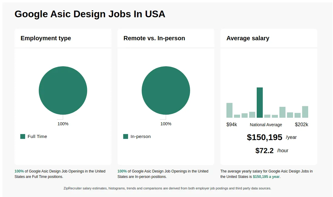
The median wage is $139.4K / yr.
$133.3K - $143.1K
33% of jobs
$143.1K - $152.9K
3% of jobs
$152.9K - $162.7K
2% of jobs
$169.2K is the 75th percentile. Wages above this are outliers.
$162.7K - $172.5K
12% of jobs
$172.5K - $182.4K
5% of jobs
$182.4K - $192.2K
4% of jobs
$192.2K - $202K
12% of jobs
$94K
$150.2K
$202K
How much do google asic design jobs pay per year?
As of Sep 12, 2026, the average yearly pay for google asic design in the United States is $150,195.00, according to ZipRecruiter salary data. Most workers in this role earn between $131,500.00 and $180,000.00 per year, depending on experience, location, and employer.
What is a Google ASIC Design?
A Google ASIC Design job involves developing custom application-specific integrated circuits (ASICs) to optimize performance, power efficiency, and functionality for Google's hardware infrastructure. Engineers in this role work on architecture, design, verification, and testing of ASICs used in data centers, AI accelerators, and other specialized hardware. They collaborate with cross-functional teams to refine system requirements and ensure successful silicon implementation. Strong expertise in digital design, hardware description languages (HDLs) like Verilog or VHDL, and synthesis tools is essential.
What does a Google ASIC Design engineer do?
As a Google ASIC Design engineer, your daily responsibilities typically involve defining microarchitectures, designing and verifying digital circuits, running design simulations, and collaborating closely with verification, software, and hardware teams. You’ll use advanced EDA tools to implement and optimize circuits, ensuring they meet strict specifications for power, performance, and area. Regular design reviews, cross-functional brainstorming sessions, and debugging activities are part of the routine. This collaborative environment fosters continual learning and innovation, providing opportunities for both technical growth and career advancement.
What are the key skills and qualifications needed to thrive in the Google ASIC Design position?
To thrive as a Google ASIC Design engineer, you need a solid background in electrical engineering, digital logic design, and experience with ASIC design methodologies. Proficiency with industry-standard EDA tools such as Synopsys, Cadence, or Mentor Graphics, along with scripting languages like Python or TCL, is essential, and a relevant certification or advanced degree can be advantageous. Strong analytical thinking, teamwork, and clear communication skills are highly valued in this role. These skills ensure high-quality, efficient chip designs that meet rigorous performance, power, and area requirements within a collaborative and fast-paced environment.
More about Google Asic Design jobs
What cities are hiring for Google Asic Design jobs?
Cities with the most Google Asic Design job openings:
What states have the most Google Asic Design jobs?
States with the most job openings for Google Asic Design jobs include:
What job categories do people searching Google Asic Design jobs look for?
The top searched job categories for Google Asic Design jobs are:
What other helpful pages are available for Google Asic Design?
Other pages related to Google Asic Design:

Static Timing Analysis Engineer, Full Chip STA
Mountain View, CA • On-site
Google Inc.
• Software Development • 10K+ employees10,000+ employees
Other
Re-posted 17 days ago
Google rating

8.8
Based on 103 frontline employees who took The Breakroom Quiz
Job description
Static Timing Analysis Engineer, Full Chip STA
#J-18808-Ljbffr- link Copy link
corporate_fare Google place Mountain View, CA, USA
MidExperience driving progress, solving problems, and mentoring more junior team members; deeper expertise and applied knowledge within relevant area.
- link Copy link
- Bachelor's degree in Electrical Engineering or Computer Science, or equivalent practical experience.
- 8 years of technical experience in silicon timing closure and chip integration.
- Experience in one or more static timing tools (e.g., PrimeTime, Tempus).
- Experience with STA signoff constraint authoring for full-chip level, tapeout signoff requirements, checklists, and associated automation.
- Master's degree in Electrical Engineering, Computer Science, or a related field.
- Experience in extraction of design parameters, QoR metrics, and analyzing data trends.
- Experience with ASIC design flows and methodology of static timing analysis.
- Knowledge of semiconductor device physics and transistor characteristics.
- Ability to deliver high complexity silicon in technology process nodes.
- Effective skills with scripting languages such as Tcl or Perl.
Be part of a team that pushes boundaries, developing custom silicon solutions that power the future of Google's direct-to-consumer products. You'll contribute to the innovation behind products loved by millions worldwide. Your expertise will shape the next generation of hardware experiences, delivering unparalleled performance, efficiency, and integration.
Google's mission is to organize the world's information and make it universally accessible and useful. Our team combines the best of Google AI, Software, and Hardware to create radically helpful experiences. We research, design, and develop new technologies and hardware to make computing faster, seamless, and more powerful. We aim to make people's lives better through technology.
Individual pay is determined by factors including job-related skills, experience, and relevant education or training.
US: $163000 - $236000 (USD) + 15% bonus target + equity + benefits
Learn more about benefits at Google .
- Define SoC timing signoff process corners, derates, uncertainties and their tradeoffs.
- Drive clock tree Jitter and implementation for SoCs to achieve best energy, performance and area.
- Manage full chip timing constraint validation, timing signoff checklist criteria, perform full chip STA, timing ECO creation and oversee final timing signoff for SoC’s.
Google is proud to be an equal opportunity and affirmative action employer. We are committed to building a workforce that is representative of the users we serve, creating a culture of belonging, and providing an equal employment opportunity regardless of race, creed, color, religion, gender, sexual orientation, gender identity/expression, national origin, disability, age, genetic information, veteran status, marital status, pregnancy or related condition (including breastfeeding), expecting or parents-to-be, criminal histories consistent with legal requirements, or any other basis protected by law. See also Google's EEO Policy , Know your rights: workplace discrimination is illegal , Belonging at Google , and How we hire .
Google is a global company and, in order to facilitate efficient collaboration and communication globally, English proficiency is a requirement for all roles unless stated otherwise in the job posting.
Equity is granted exclusively and discretionarily by Alphabet Inc. on the basis of an agreement concluded between you and Alphabet Inc. Alphabet Inc. is your sole contractual partner with respect to equity grants. GSU grants are not guaranteed, are discretionary, are subject to approval by the Alphabet Inc. board of directors or its delegate, the terms of the relevant Alphabet Inc. stock plan, and your grant agreement. They have no impact on statutory payments. Current or past grants do not confer an acquired right.

About Google
Sourced by ZipRecruiter
Industry
Software development and technology, communication and media
Company size
10,000+ Employees
Headquarters location
Mountain View, CA, US