Understanding of semiconductor device physics and packaging process technologies. * Strong ... advanced packaging and 3DIC technologies. You will collaborate with world-class engineers, work on ...
Understanding of semiconductor device physics and packaging process technologies. * Strong ... advanced packaging and 3DIC technologies. You will collaborate with world-class engineers, work on ...
Process Integration Engineer E4
$128K - $176K/yr
As a Process Engineer, you'll play a crucial role in designing and optimizing manufacturing ... Work with advanced packaging, process, hardware, and metrology team to develop new materials ...
Process Integration Engineer E4
$128K - $176K/yr
As a Process Engineer, you'll play a crucial role in designing and optimizing manufacturing ... Work with advanced packaging, process, hardware, and metrology team to develop new materials ...

As a Principal Engineer (Hardware), Advanced Packaging, you will play a key role in advancing ASM's semiconductor process technologies. You'll leverage your expertise in thin-film deposition and ...
As a Principal Engineer (Hardware), Advanced Packaging, you will play a key role in advancing ASM's semiconductor process technologies. You'll leverage your expertise in thin-film deposition and ...

Process Integration Engineer E4
Albany, NY · On-site
$128K - $176K/yr
As a Process Engineer, you'll play a crucial role in designing and optimizing manufacturing ... Work with advanced packaging, process, hardware, and metrology team to develop new materials ...
Process Integration Engineer E4
Albany, NY · On-site
$128K - $176K/yr
As a Process Engineer, you'll play a crucial role in designing and optimizing manufacturing ... Work with advanced packaging, process, hardware, and metrology team to develop new materials ...
Advanced Packaging Microelectronics Integration Engineer - Fan Out
Kissimmee, FL · On-site
$158.96K - $238.44K/yr
We are looking for a hardworking, and passionate experienced Sr. Process Integration and Development Engineer for our Florida Advanced Packaging site. In this role, you will lead, develop, and ...
Advanced Packaging Microelectronics Integration Engineer - Fan Out
Kissimmee, FL · On-site
$158.96K - $238.44K/yr
We are looking for a hardworking, and passionate experienced Sr. Process Integration and Development Engineer for our Florida Advanced Packaging site. In this role, you will lead, develop, and ...
Advanced Packaging Microelectronics Integration Engineer - Fan Out
$158.96K - $238.44K/yr
We are looking for a hardworking, and passionate experienced Sr. Process Integration and Development Engineer for our Florida Advanced Packaging site. In this role, you will lead, develop, and ...
Advanced Packaging Microelectronics Integration Engineer - Fan Out
$158.96K - $238.44K/yr
We are looking for a hardworking, and passionate experienced Sr. Process Integration and Development Engineer for our Florida Advanced Packaging site. In this role, you will lead, develop, and ...
Advanced Packaging Integration Engineer
Santa Clara, CA · On-site
$138K - $190K/yr
As an Advanced Packaging Integration Engineer , you will lead process integration for high-performance interconnects and microLED panels. You will architect robust, scalable integration flows that ...
Advanced Packaging Integration Engineer
Santa Clara, CA · On-site
$138K - $190K/yr
As an Advanced Packaging Integration Engineer , you will lead process integration for high-performance interconnects and microLED panels. You will architect robust, scalable integration flows that ...
Advanced Packaging Engineer
Saratoga, CA · On-site
$230K - $275K/yr
Position Overview We are seeking a highly experienced Advanced Package Engineer to lead system ... Evaluate PCB SMT rework processes using real sample parts and production data. * Define and ...
Advanced Packaging Engineer
Saratoga, CA · On-site
$230K - $275K/yr
Position Overview We are seeking a highly experienced Advanced Package Engineer to lead system ... Evaluate PCB SMT rework processes using real sample parts and production data. * Define and ...
Advanced Packaging Integration Engineer
Santa Clara, CA · On-site
$176K - $242K/yr
As an Advanced Packaging Integration Engineer, you will lead process integration for high-performance interconnects and microLED panels. You will architect robust, scalable integration flows that ...
Advanced Packaging Integration Engineer
Santa Clara, CA · On-site
$176K - $242K/yr
As an Advanced Packaging Integration Engineer, you will lead process integration for high-performance interconnects and microLED panels. You will architect robust, scalable integration flows that ...
Advanced Packaging Integration Engineer
Santa Clara, CA · Hybrid
$176K - $242K/yr
As an Advanced Packaging Integration Engineer, you will lead process integration for high-performance interconnects and microLED panels. You will architect robust, scalable integration flows that ...
Advanced Packaging Integration Engineer
Santa Clara, CA · Hybrid
$176K - $242K/yr
As an Advanced Packaging Integration Engineer, you will lead process integration for high-performance interconnects and microLED panels. You will architect robust, scalable integration flows that ...
Advanced Packaging Integration Engineer
Santa Clara, CA · Hybrid
$138K - $190K/yr
As an Advanced Packaging Integration Engineer , you will lead process integration for highperformance interconnects and microLED panels. You will architect robust, scalable integration flows that ...
Advanced Packaging Integration Engineer
Santa Clara, CA · Hybrid
$138K - $190K/yr
As an Advanced Packaging Integration Engineer , you will lead process integration for highperformance interconnects and microLED panels. You will architect robust, scalable integration flows that ...

Sr. Silicon Packaging Process Engineer, Silicon Technology (Starlink)
Bastrop, TX · On-site
$103.40K - $133.80K/yr
... PROCESS ENGINEER, SILICON TECHNOLOGY (STARLINK) SpaceX is leveraging its experience in building ... Advanced technical degree * 7+ years industry experience with microelectronics packaging ...
Sr. Silicon Packaging Process Engineer, Silicon Technology (Starlink)
Bastrop, TX · On-site
$103.40K - $133.80K/yr
... PROCESS ENGINEER, SILICON TECHNOLOGY (STARLINK) SpaceX is leveraging its experience in building ... Advanced technical degree * 7+ years industry experience with microelectronics packaging ...
Advanced Packaging Integration Engineer
Santa Clara, CA · On-site
$161K - $221K/yr
As an Advanced Packaging Integration Engineer , you will lead process integration for high-performance interconnects and microLED panels. You will architect robust, scalable integration flows that ...
Advanced Packaging Integration Engineer
Santa Clara, CA · On-site
$161K - $221K/yr
As an Advanced Packaging Integration Engineer , you will lead process integration for high-performance interconnects and microLED panels. You will architect robust, scalable integration flows that ...
Advanced Packaging Integration Engineer
Santa Clara, CA · Hybrid
$161K - $221K/yr
As an Advanced Packaging Integration Engineer , you will lead process integration for highperformance interconnects and microLED panels. You will architect robust, scalable integration flows that ...
Advanced Packaging Integration Engineer
Santa Clara, CA · Hybrid
$161K - $221K/yr
As an Advanced Packaging Integration Engineer , you will lead process integration for highperformance interconnects and microLED panels. You will architect robust, scalable integration flows that ...

... Engineering, Materials Science, Physics, Chemistry, or relevant fields coupled with 2-5+ years of applicable experience in semiconductor fabrication/advanced packaging processes. We are seeking an ...
... Engineering, Materials Science, Physics, Chemistry, or relevant fields coupled with 2-5+ years of applicable experience in semiconductor fabrication/advanced packaging processes. We are seeking an ...
... Engineering, Materials Science, Physics, Chemistry, or relevant fields coupled with 2-5+ years of applicable experience in semiconductor fabrication/advanced packaging processes. We are seeking an ...
... Engineering, Materials Science, Physics, Chemistry, or relevant fields coupled with 2-5+ years of applicable experience in semiconductor fabrication/advanced packaging processes. We are seeking an ...

Senior Optical Packaging Process Engineer
$121.20K - $156.70K/yr
By leveraging the advanced semiconductor manufacturing industry-including partners like ... Lead process development and qualification for optical module packaging. * Support NPI efforts ...
Senior Optical Packaging Process Engineer
$121.20K - $156.70K/yr
By leveraging the advanced semiconductor manufacturing industry-including partners like ... Lead process development and qualification for optical module packaging. * Support NPI efforts ...
Senior Optical Packaging Process Engineer
$118.60K - $153.30K/yr
Byleveragingthe advanced semiconductor manufacturing industry-including partners like ... Lead process development and qualification for optical module packaging. * Support NPI efforts ...
Senior Optical Packaging Process Engineer
$118.60K - $153.30K/yr
Byleveragingthe advanced semiconductor manufacturing industry-including partners like ... Lead process development and qualification for optical module packaging. * Support NPI efforts ...
Senior Optical Packaging Process Engineer
Milpitas, CA · On-site
$121.20K - $156.70K/yr
By leveraging the advanced semiconductor manufacturing industry-including partners like ... Lead process development and qualification for optical module packaging. * Support NPI efforts ...
Senior Optical Packaging Process Engineer
Milpitas, CA · On-site
$121.20K - $156.70K/yr
By leveraging the advanced semiconductor manufacturing industry-including partners like ... Lead process development and qualification for optical module packaging. * Support NPI efforts ...

Packaging Module Engineer
Phoenix, AZ · On-site
Lead packaging development processes, including artwork creation, concepts, prototypes ... advanced packaging all the way to final test and assembly. We ensure our foundry customers ...
Packaging Module Engineer
Phoenix, AZ · On-site
Lead packaging development processes, including artwork creation, concepts, prototypes ... advanced packaging all the way to final test and assembly. We ensure our foundry customers ...
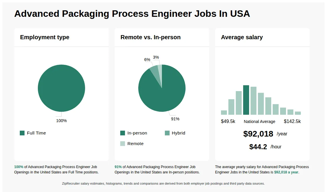
Advanced Packaging Process Engineer information
See salary details
$49.5K - $58K
2% of jobs
$58K - $66.4K
9% of jobs
$74.1K is the 25th percentile. Wages below this are outliers.
$66.4K - $74.9K
15% of jobs
$74.9K - $83.3K
18% of jobs
The median wage is $86.2K / yr.
$83.3K - $91.8K
17% of jobs
$91.8K - $100.2K
14% of jobs
$100.4K is the 75th percentile. Wages above this are outliers.
$100.2K - $108.7K
11% of jobs
$108.7K - $117.1K
6% of jobs
$117.1K - $125.6K
4% of jobs
$125.6K - $134K
3% of jobs
$134K - $142.5K
1% of jobs
$49.5K
$92K
$142.5K
How much do advanced packaging process engineer jobs pay per year?
As of May 31, 2026, the average yearly pay for advanced packaging process engineer in the United States is $92,018.00, according to ZipRecruiter salary data. Most workers in this role earn between $74,500.00 and $103,000.00 per year, depending on experience, location, and employer.
What are the key skills and qualifications needed to thrive as an Advanced Packaging Process Engineer, and why are they important?
To thrive as an Advanced Packaging Process Engineer, you need a strong background in materials science, semiconductor manufacturing, and process optimization, usually backed by a relevant engineering degree. Familiarity with tools such as AutoCAD, failure analysis equipment, and process control systems, as well as knowledge of standards like IPC and JEDEC, is typically required. Strong problem-solving, attention to detail, and effective communication skills help engineers collaborate across teams and address complex technical challenges. These skills and qualities are crucial for ensuring innovative, reliable, and cost-effective semiconductor packaging solutions.
What are some common challenges faced by Advanced Packaging Process Engineers in the transition from R&D to high-volume manufacturing?
Advanced Packaging Process Engineers often encounter challenges when scaling up new packaging technologies from research and development to high-volume manufacturing. These challenges include ensuring process stability, maintaining yield and quality standards, and integrating new processes with existing production lines. Engineers must closely collaborate with cross-functional teams such as design, quality assurance, and equipment maintenance to resolve issues quickly and meet production targets. Continuous optimization and troubleshooting are key aspects of the role, requiring strong problem-solving skills and adaptability.
What is an Advanced Packaging Process Engineer?
An Advanced Packaging Process Engineer is a specialized professional in the semiconductor industry who focuses on developing and optimizing the processes used to assemble and package microchips and electronic components. Their work includes designing and improving advanced packaging technologies such as 2.5D/3D integration, wafer-level packaging, and system-in-package (SiP) solutions. They ensure high performance, reliability, and manufacturability of the final products by collaborating with cross-functional teams in engineering, manufacturing, and quality assurance. This role is crucial for meeting the industry's demands for smaller, faster, and more efficient electronic devices.
What is the difference between Advanced Packaging Process Engineer vs Packaging Engineer?
| Aspect | Advanced Packaging Process Engineer | Packaging Engineer |
|---|---|---|
| Credentials | Bachelor's or higher in Engineering, certifications like IPC or Six Sigma | Bachelor's in Engineering or related field, certifications vary |
| Work Environment | Semiconductor, electronics manufacturing, R&D labs | Consumer goods, industrial products, manufacturing facilities |
| Industry Usage | High-tech electronics, semiconductor industry | Consumer products, packaging design and production |
| Job Focus | Developing advanced packaging processes, improving yield and reliability | Designing, testing, and implementing packaging solutions |
The Advanced Packaging Process Engineer specializes in developing and optimizing complex packaging processes for high-tech industries like semiconductors, focusing on innovation and reliability. In contrast, the Packaging Engineer typically works on designing and managing packaging solutions for consumer and industrial products. While both roles require engineering knowledge and certifications, their industry focus and daily tasks differ significantly.
Full-time
Posted 3 days ago
TSMC rating

8.2
Based on 19 frontline employees who took The Breakroom Quiz
36th of 137 rated electronics manufacturers
Job description
Context
As chip sizes increase and packaging technologies become more complex, substrate engineering is emerging as a critical domain. This role supports TSMC's leadership in 3DIC and advanced packaging by extending expertise beyond chip-level design into package-level integration. The team is addressing challenges such as warpage, power delivery, thermal management, and material innovation. Future evolution includes Chip-on-Wafer-on-PCB (CoWoP) under TSMC's System Technology Optimization program.
The position requires strong design and technology expertise to define future customer requirements, focusing on integrated packaging (IP), dielectric parameters, high-speed I/O, and trade-offs that directly impact system performance. This role is critical in shaping the direction of 3DIC development.
Overview
We are seeking a highly skilled and motivated Substrate / Advanced Package Engineer to join our cutting-edge 3DIC design team. The ideal candidate will have a strong foundation in semiconductor physics, mechanical engineering principles, and EDA (Electronic Design Automation) tools, with a passion for innovation in advanced package design. The role involves design, simulation, and modeling of complex substrate and packaging technologies to support next generation 3DIC applications.
Responsibilities
Requirements
Preferred Skills
Success Metrics
Location
Why TSMC?
At TSMC, you will be part of the world's leading semiconductor foundry, driving cutting-edge innovation in advanced packaging and 3DIC technologies. You will collaborate with world-class engineers, work on industry-defining projects, and shape the future of system integration. We offer unparalleled opportunities for growth, impact, and contribution to the global technology ecosystem.
Company Description
As a trusted technology and capacity provider, TSMC is driven by the desire to be:
TSMC pioneered the pure-play foundry business model when it was founded in 1987 and has been the world's leading dedicated semiconductor foundry ever since. The Company supports a thriving ecosystem of global customers and partners with the industry's leading process technologies and a portfolio of design enablement solutions to unleash innovation for the global semiconductor industry. With global operations spanning Asia, Europe, and North America, TSMC serves as a committed corporate citizen around the world.
In North America, TSMC has a strong sales and service organization that works with customers by helping them achieve silicon success with cutting-edge technologies and manufacturing excellence. The Company has continued to accelerate its R&D investment and staffing in recent years and is expanding its manufacturing footprint to support customer innovation with 3D IC technologies and optimal manufacturing capacity.
For positions requiring access to technical data subject to export control regulations, including Export Administration Regulations, TSMC North America may have to obtain export licensing approval from the U.S. Government for certain individuals. All employment is contingent upon TSMC North America obtaining any export license or other approval that may be required by the U.S. Government.
Diversity statement
TSMC Technology, Inc. is committed to employing a diverse workforce and provides Equal Employment Opportunity for all individuals regardless of race, color, religion, gender, age, national origin, marital status, sexual orientation, gender identity, status as a protected veteran, genetic information, or any other characteristic protected by applicable law.
TSMC is an equal opportunity employer prizing diversity and inclusion. We are committed to treating all employees and applicants for employment with respect and dignity. If you require reasonable accommodation due to a disability during the application or the recruiting process, please feel free to notify us at G_ACCOMMODATIONS@TSMC.COM. TSMC confirms to all applicants its commitment to meet TSMC's obligations under applicable employment law. Reasonable accommodations will be determined on a case-by-case basis.
Pay Transparency / Benefits statement
At TSMC, your base pay is only part of your overall total compensation package. At the time of this posting, this role typically pays a base salary between $153,500 and $250,000 per year. The range displayed reflects the minimum and maximum target for new hires. Actual pay may be more or less than the posted range. Factors that influence pay include the individual's skills, qualifications, education, experience and the position level and location. TSMC's total compensation package consists of market competitive pay, allowances, bonuses, and comprehensive benefits. We also offer extensive development opportunities and programs.
For roles hired outside of California, including other U.S. states or international locations such as Taiwan, compensation may vary in accordance with local market practices, legal requirements, and TSMC's regional compensation framework.
Date: May 19, 2026
Country/Region: US
City: San Jose
Company: TSMC Technology, Inc.
As chip sizes increase and packaging technologies become more complex, substrate engineering is emerging as a critical domain. This role supports TSMC's leadership in 3DIC and advanced packaging by extending expertise beyond chip-level design into package-level integration. The team is addressing challenges such as warpage, power delivery, thermal management, and material innovation. Future evolution includes Chip-on-Wafer-on-PCB (CoWoP) under TSMC's System Technology Optimization program.
The position requires strong design and technology expertise to define future customer requirements, focusing on integrated packaging (IP), dielectric parameters, high-speed I/O, and trade-offs that directly impact system performance. This role is critical in shaping the direction of 3DIC development.
Overview
We are seeking a highly skilled and motivated Substrate / Advanced Package Engineer to join our cutting-edge 3DIC design team. The ideal candidate will have a strong foundation in semiconductor physics, mechanical engineering principles, and EDA (Electronic Design Automation) tools, with a passion for innovation in advanced package design. The role involves design, simulation, and modeling of complex substrate and packaging technologies to support next generation 3DIC applications.
Responsibilities
- Design, simulate, and optimize advanced packaging for 3DIC applications.
- Collaborate with cross-functional teams to define specifications and requirements.
- Perform modeling of warpage, stress, reliability, and thermal performance using industry-standard EDA tools.
- Formulate and solve problems in research-driven, often ambiguous domains.
- Provide guidance on high-speed I/O modeling and integration.
- Develop and maintain documentation, including specifications, test plans, and design reviews.
Stay current with industry trends, tools, and technologies in advanced packaging.
Requirements
- Master's degree or Ph.D. in Electrical Engineering, Mechanical Engineering, or a related field.
- 15+ years of hands-on expertise in advanced packaging technologies and substrate design.
- Understanding of semiconductor device physics and packaging process technologies.
- Strong knowledge of warpage, stress, and thermal effects in packaging.
- Proven ability to drive solutions in ambiguous, research-oriented contexts.
- Excellent problem-solving, analytical, and communication skills.
- Strong collaboration skills, with the ability to mentor junior engineers.
- Ability to balance strategic insight with hands-on technical execution.
Preferred Skills
- Experience with reliability, IR/EM, and multi-physics analysis.
- Familiarity with machine learning techniques for design optimization.
- Patents, publications, or demonstrated innovation in substrate or packaging domains.
Success Metrics
- Ability to provide impactful, data-driven suggestions that influence design direction.
- Effective use of modeling and simulation to validate proposals.
- Establishing trust and credibility with global teams.
- Enabling adoption of new technologies within the 3DIC ecosystem.
Location
- San Jose, CA or Hsinchu, Taiwan.
Why TSMC?
At TSMC, you will be part of the world's leading semiconductor foundry, driving cutting-edge innovation in advanced packaging and 3DIC technologies. You will collaborate with world-class engineers, work on industry-defining projects, and shape the future of system integration. We offer unparalleled opportunities for growth, impact, and contribution to the global technology ecosystem.
Company Description
As a trusted technology and capacity provider, TSMC is driven by the desire to be:
- The world's leading dedicated semiconductor foundry
- The technology leader with a strong reputation for manufacturing excellence
- Advancing semiconductor manufacturing innovations to enable the future of technology
TSMC pioneered the pure-play foundry business model when it was founded in 1987 and has been the world's leading dedicated semiconductor foundry ever since. The Company supports a thriving ecosystem of global customers and partners with the industry's leading process technologies and a portfolio of design enablement solutions to unleash innovation for the global semiconductor industry. With global operations spanning Asia, Europe, and North America, TSMC serves as a committed corporate citizen around the world.
In North America, TSMC has a strong sales and service organization that works with customers by helping them achieve silicon success with cutting-edge technologies and manufacturing excellence. The Company has continued to accelerate its R&D investment and staffing in recent years and is expanding its manufacturing footprint to support customer innovation with 3D IC technologies and optimal manufacturing capacity.
For positions requiring access to technical data subject to export control regulations, including Export Administration Regulations, TSMC North America may have to obtain export licensing approval from the U.S. Government for certain individuals. All employment is contingent upon TSMC North America obtaining any export license or other approval that may be required by the U.S. Government.
Diversity statement
TSMC Technology, Inc. is committed to employing a diverse workforce and provides Equal Employment Opportunity for all individuals regardless of race, color, religion, gender, age, national origin, marital status, sexual orientation, gender identity, status as a protected veteran, genetic information, or any other characteristic protected by applicable law.
TSMC is an equal opportunity employer prizing diversity and inclusion. We are committed to treating all employees and applicants for employment with respect and dignity. If you require reasonable accommodation due to a disability during the application or the recruiting process, please feel free to notify us at G_ACCOMMODATIONS@TSMC.COM. TSMC confirms to all applicants its commitment to meet TSMC's obligations under applicable employment law. Reasonable accommodations will be determined on a case-by-case basis.
Pay Transparency / Benefits statement
At TSMC, your base pay is only part of your overall total compensation package. At the time of this posting, this role typically pays a base salary between $153,500 and $250,000 per year. The range displayed reflects the minimum and maximum target for new hires. Actual pay may be more or less than the posted range. Factors that influence pay include the individual's skills, qualifications, education, experience and the position level and location. TSMC's total compensation package consists of market competitive pay, allowances, bonuses, and comprehensive benefits. We also offer extensive development opportunities and programs.
For roles hired outside of California, including other U.S. states or international locations such as Taiwan, compensation may vary in accordance with local market practices, legal requirements, and TSMC's regional compensation framework.
Date: May 19, 2026
Country/Region: US
City: San Jose
Company: TSMC Technology, Inc.