1

Advanced Packaging Process Engineer Jobs (NOW HIRING)

NY Creates also runs some of the most advanced facilities in the world, boasts more than 3,000 ... Position Summary, Packaging Process Engineer NY Creates is looking for a Packaging Process Engineer ...

Senior Process Engineer

Gardena, CA ยท On-site

$140K - $180K/yr

... packaging, assembly, or advanced manufacturing environments * Demonstrated success qualifying ... Senior Process Engineer: $140,000.00 - $180,000.00/per year Title and base salary are determined on ...

Senior Process Engineer

Gardena, CA ยท On-site

$140K - $180K/yr

... packaging, assembly, or advanced manufacturing environments * Demonstrated success qualifying ... Senior Process Engineer: $140,000.00 - $180,000.00/per year Title and base salary are determined on ...

next page

Showing results 1-20

Advanced Packaging Process Engineer information

See salary details

$49.5K

$92K

$142.5K

How much do advanced packaging process engineer jobs pay per year?

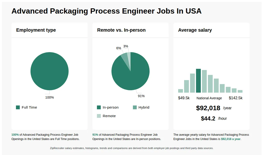
As of May 31, 2026, the average yearly pay for advanced packaging process engineer in the United States is $92,018.00, according to ZipRecruiter salary data. Most workers in this role earn between $74,500.00 and $103,000.00 per year, depending on experience, location, and employer.

What are the key skills and qualifications needed to thrive as an Advanced Packaging Process Engineer, and why are they important?

To thrive as an Advanced Packaging Process Engineer, you need a strong background in materials science, semiconductor manufacturing, and process optimization, usually backed by a relevant engineering degree. Familiarity with tools such as AutoCAD, failure analysis equipment, and process control systems, as well as knowledge of standards like IPC and JEDEC, is typically required. Strong problem-solving, attention to detail, and effective communication skills help engineers collaborate across teams and address complex technical challenges. These skills and qualities are crucial for ensuring innovative, reliable, and cost-effective semiconductor packaging solutions.

What are some common challenges faced by Advanced Packaging Process Engineers in the transition from R&D to high-volume manufacturing?

Advanced Packaging Process Engineers often encounter challenges when scaling up new packaging technologies from research and development to high-volume manufacturing. These challenges include ensuring process stability, maintaining yield and quality standards, and integrating new processes with existing production lines. Engineers must closely collaborate with cross-functional teams such as design, quality assurance, and equipment maintenance to resolve issues quickly and meet production targets. Continuous optimization and troubleshooting are key aspects of the role, requiring strong problem-solving skills and adaptability.

What is an Advanced Packaging Process Engineer?

An Advanced Packaging Process Engineer is a specialized professional in the semiconductor industry who focuses on developing and optimizing the processes used to assemble and package microchips and electronic components. Their work includes designing and improving advanced packaging technologies such as 2.5D/3D integration, wafer-level packaging, and system-in-package (SiP) solutions. They ensure high performance, reliability, and manufacturability of the final products by collaborating with cross-functional teams in engineering, manufacturing, and quality assurance. This role is crucial for meeting the industry's demands for smaller, faster, and more efficient electronic devices.

What is the difference between Advanced Packaging Process Engineer vs Packaging Engineer?

AspectAdvanced Packaging Process EngineerPackaging Engineer
CredentialsBachelor's or higher in Engineering, certifications like IPC or Six SigmaBachelor's in Engineering or related field, certifications vary
Work EnvironmentSemiconductor, electronics manufacturing, R&D labsConsumer goods, industrial products, manufacturing facilities
Industry UsageHigh-tech electronics, semiconductor industryConsumer products, packaging design and production
Job FocusDeveloping advanced packaging processes, improving yield and reliabilityDesigning, testing, and implementing packaging solutions

The Advanced Packaging Process Engineer specializes in developing and optimizing complex packaging processes for high-tech industries like semiconductors, focusing on innovation and reliability. In contrast, the Packaging Engineer typically works on designing and managing packaging solutions for consumer and industrial products. While both roles require engineering knowledge and certifications, their industry focus and daily tasks differ significantly.

Infographic showing various Advanced Packaging Process Engineer job openings in the United States as of May 2026, with employment types broken down into 100% Full Time. Highlights an 100% In-person job distribution, with an average salary of $92,018 per year, or $44.2 per hour.

Advanced Packaging Process Engineer

Tenstorrent

Santa Clara, CA โ€ข Hybrid

$100K - $500K/yr

Other

Posted 24 days ago


Job description

Tenstorrent is seeking an Advanced Packaging Process Engineer with experience in 2.5D and 3D chiplet packaging to join Tenstorrent's Packaging team. You will drive advanced package technology and reliability in close partnership with foundries and OSATs, helping push performance and manufacturability for nextgeneration AI/ML products.

This role is hybrid, based out of Santa Clara, CA or Taipei City, TW.

We welcome candidates at various experience levels for this role. During the interview process, candidates will be assessed for the appropriate level, and offers will align with that level, which may differ from the one in this posting.

Who you areย 

  • Advanced packaging engineer with hands-on 2.5D/3D experience (CoWoS-R/L, FOCoS, EMIB, FCBGA, organic substrates, silicon interposers, embedded Si/eCB, micro-bumps, BGAs).
  • Strong in reliability and failure analysis for advanced packaging, including qualification, root cause analysis, and corrective actions.
  • Deep understanding of process flows and materials (polyimide, ABF, core, underfill, mold compound) and their interactions (warpage, stress, delamination, mechanical risk).
  • Proven track record working with foundries/OSATs on NPI, design rules, excursions, yield/cost optimization, and production ramp, with clear communication and cross-functional collaboration.

What we needย 

  • Own advanced package technology implementation for 2.5D/3D chiplet products, including technology choices, process integration, and manufacturability.
  • Act as primary technical interface to foundries/OSATs: align capabilities and design rules, manage excursions, drive yield, define/track test vehicles, and coordinate FA.
  • Partner with design, reliability, and architecture teams to evaluate tradeoffs (bump pitch, stack-ups, embedded Si, etc.) and lead test vehicle planning to meet program needs.
  • MS/PhD in a relevant field (Materials, Mechanical, Electrical, Physics, or related) and 5+ years in advanced packaging for high-performance semiconductors from NPI through production (2.5D/3D flows such as CoWoS, FOCoS, EMIB, FCBGA or equivalent).

What you will learnย 

  • Deeper exposure to leading-edge 2.5D/3D packaging for high-performance AI/ML and chiplet-based architectures.
  • How to balance performance-driven architecture with mechanical and reliability constraints to make robust package technology decisions.
  • Ways to use AI- and automation-driven methods to accelerate risk assessment, qualification planning, and technical documentation.
  • Best practices for building strategic OSAT and foundry partnerships that enable new capabilities while scaling reliable high-volume production.

Compensation for all engineers at Tenstorrent ranges from $100k - $500k including base and variable compensation targets. Experience, skills, education, background and location all impact the actual offer made.

Tenstorrent offers a highly competitive compensation package and benefits, and we are an equal opportunity employer.